高密度功率模块简化和缩小电动汽车电源系统设计
Vicor 电源模块为电动汽车应用注入创新。了解三款汽车级新产品将如何彻底改变未来的电源设计
Buck voltage regulation, an essential part of distributing power from a DC supply to its points of load (PoLs), has typically been implemented with a PWM circuit. The PWM duty cycle is varied to accommodate the required voltage reduction.
However a couple of factors have applied increasing pressure to regulator design. Firstly, power density is being forced up as continuously more powerful devices are designed onto boards without corresponding increase in footprint. Secondly, DC power supply voltage levels are tending to rise to minimize distribution losses, while device voltages are reducing to increase internal speed and efficiency. These trends combine to increase the voltage drop and associated switching losses across the regulator.
For example a process control system may call for regulation from 24V to 3.3V – a gap that would typically be covered using two regulation stages; increasing board space, cost and reliability issues. The regulator’s switching frequency is also limited, as increased switching activity incurs more losses. This in turn limits the use of smaller passive components for filtering, penalizing the density of the total solution.
Although high-density PWM regulators have evolved with improved IC integration, MOSFETs and packaging, their design is no longer sufficient to meet the power demands they face. This is mainly due to switching losses within the regulator MOSFETs. These must be overcome or avoided to achieve any significant boost to regulator performance.
A better solution uses zero-voltage-switching (ZVS) topology, which allows for operation at a higher frequency and at higher input voltages without sacrificing efficiency. While still PWM based, a separate phase is added to the PWM timing to allow for ZVS operation. Figure 1 compares a conventional buck regulator with a version modified for ZVS operation. Utilizing the added phase, the ZVS type uses the clamp switch and circuit resonance to operate the high side (Q1) and synchronous (Q2) MOSFETs efficiently with soft switching, avoiding the losses they incur during conventional PWM operation and timing.
For example in the conventional circuit, as Q1 is turned on and Q2 turned off, a very high current flows through the MOSFET pair, since Q2’s body diode appears as a short circuit during its reverse recovery time. Other losses arise due to discharging Q1’s output capacitance, and to reverse recovery in Q2. These losses increase as the switching frequency or input voltage increases.
By contrast the ZVS design addresses the high turn-on losses of the conventional regulator by eliminating high current body diode conduction prior to turn on of the high-side MOSFET, bringing the D-S voltage of the high side MOSFET to zero or nearly zero and producing no high current spikes or damaging ringing. The ZVS action applied to Q1 removes its Miller effect at turn on, allowing the use of a smaller driver and lower gate drive.
Vicor has utilized ZVS topology within our buck regulators. These provide regulation up to 36VIN at a higher efficiency and from a smaller form factor than achievable from conventional hard switching, high density regulators.
Figure 1: ZVS Buck
Figure 1: ZVS Buck
Related content
Product overview: buck regulators
高密度功率模块简化和缩小电动汽车电源系统设计
Vicor 电源模块为电动汽车应用注入创新。了解三款汽车级新产品将如何彻底改变未来的电源设计
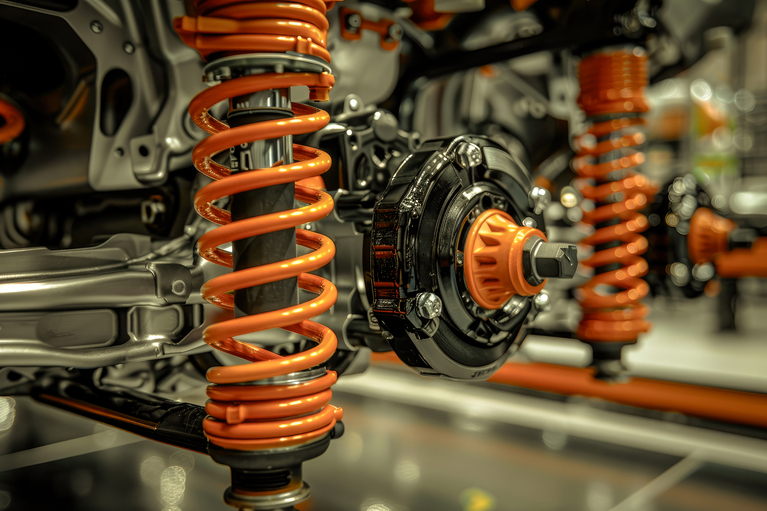
高密度电源模块推动主动悬架技术日趋成熟
主动悬挂系统已从 20 世纪 90 年代的测试版发展成为今天的 48V 驱动系统。了解电源模块对电源系统设计的影响
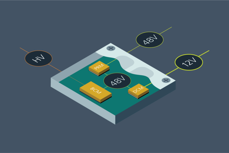
先进的电源模块封装优化了自动驾驶电动巴士的可用功率、可靠性和安全性
Vicor 的高效电源模块确保最少的散热,降低对复杂冷却解决方案的需求,并最大限度地提升功率输出
基于 MHz 开关频率的器件助力实现 DC-DC 转换器和 EMI 滤波器的小型化
想象一下,使用 DC-DC 转换器解决方案来利用高频开关的优势,而不会发生传统解決方案的缺点